https://www.pv-magazine.com/2023/12/28/optical-photovoltaic-converters-for-high-power-transmission-systems/
Optical photovoltaic converters for power transmission systems

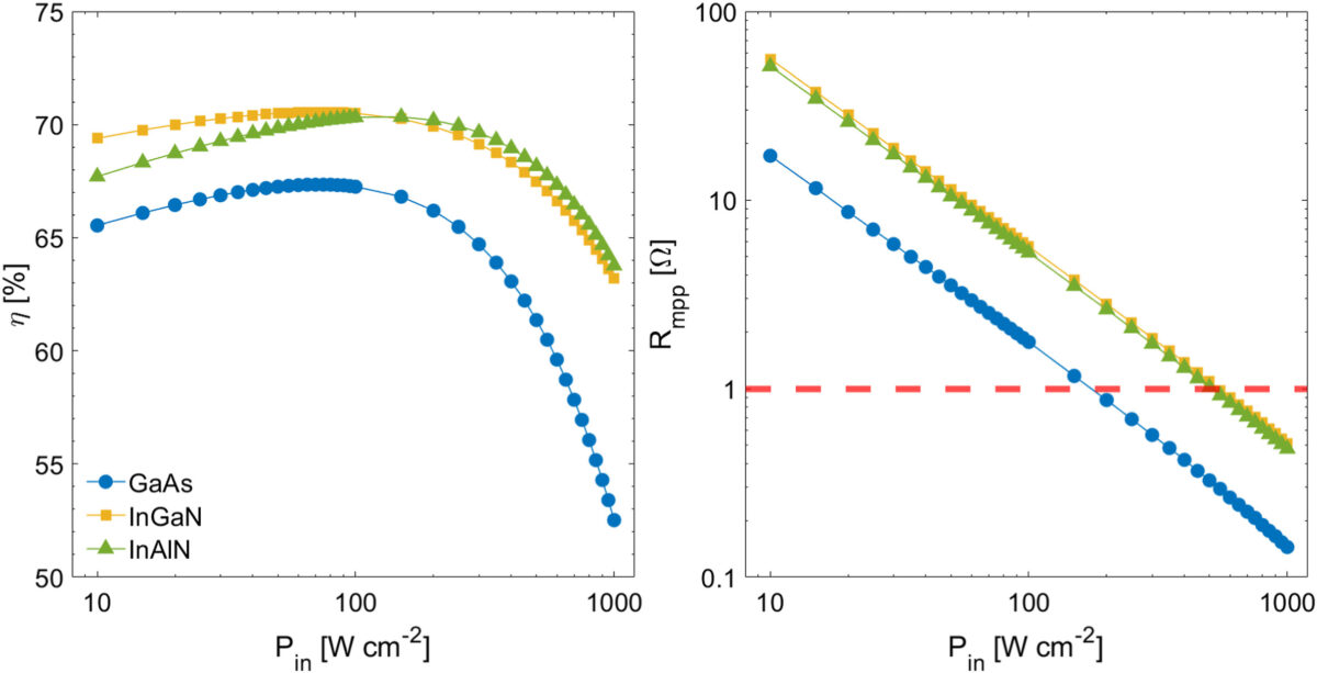
OPCs efficiencies (left) and optimal load (right)
Image: University of Jaén, Solar Energy Materials and Solar Cells, CC BY 4.0 DEED
Scientists from the University of Jaén and the University of Santiago de Compostela in Spain have conducted research to identify the most suitable semiconductor materials for high-power optical transmission (HPOT) in terrestrial and underwater environments.
HPOT, also known as laser power transmission, is an approach that uses a monochromatic light source to transfer continuous power to a remote system via an optical photovoltaic converter (OPC).
“Within the upcoming year, we aim to initiate the manufacture of OPCs based on indium gallium nitride (InGaN) and indium aluminum nitride (InAlN) as proof of concept, laying the groundwork to surpass the maximum efficiencies reported to date,” researcher Pablo Sanmartín told pv magazine.
Their modeling considered three types of recombination mechanisms and was validated by comparing the results for GaAs with empirical results from the scientific literature.
“The concordance between the obtained results is noteworthy, exhibiting relative errors that remain below 1.6% for all parameters and input power densities,” the researchers said.
The group conducted a series of tests and found that the maximum efficiencies were 67.3% at 70 Wcm-2 for GaAs, 70.6% at 75 Wcm-2 for InGaN, and 70.3% at 150 Wcm-2 for InAlN. In the atmosphere, InGaN showed the highest efficiencies within the 10 km, ranging from 70.5 to 65.3%, while InAlN displayed results from 70.3 to 65.1%. In compression, GaAs results were lower at 67.3% to 62.4%.
Popular content
The nitrides also displayed better results when the medium was water. InGaN achieved a 9.8% global efficiency at 100 meters, while InAlN did 8.6%. In contrast, GaAs presented much more inferior results, with the efficiency dropping to 2.4% at only 1 meter.
“This semiconductor is practically unusable for underwater applications,” the academics said. “It is worth noting that at a distance of 20 m, nitride-based OPCs still reach a global efficiency of over 46%.
The research group said that the nitrides could potentially produce roughly ten times more energy in the same amount of time. They exhibit high efficiencies of more than 63% at extreme light intensities of 1,000 Wcm-2. For comparison, GaAs's highest achievable efficiency is around the same as 67.3% at 100 Wcm-2.
“This enhancement is mainly attributed to the reduction of series resistance losses at intense illuminations, from 28% to around 14%, due to the decrease of current density caused by the use of higher energy gap materials,” they explained.
They described their findings in “Wide-bandgap III-V materials for high-efficiency air and underwater optical photovoltaic power transmission,” which was recently published in Solar Energy Materials and Solar Cells.
“It is worth noting that the potential fabrication of the devices is constrained to the technological manufacturing restrictions that may arise during the process, as growing the semiconductors with sufficient quality, reaching the desired doping levels or avoid lattice mismatches between the layers,” the researchers said. “The viability of the process also depends on whether the preferred wavelengths or similar are available. In addition, the monochromatic light source should be able to provide such intense power densities and guarantee an operable angular dispersion of the beam within the distances considered.”
This content is protected by copyright and may not be reused. If you want to cooperate with us and would like to reuse some of our content, please contact: editors@pv-magazine.com.


